TeraTom project funded by the National Growth Fund
5 December 2024

The building blocks of all the semiconductor devices that sustain our “society of technology” are wafers and thin films that are repeatedly grown before they go into further processing steps. At the same time, to realize new functionalities in semiconductor devices and make optimal use of available wafer space, semiconductor devices will shrink to even atomic scale, using novel materials, while being designed in 3D-configurations. Necessity for pre-inspection and in-line characterization of materials on a very detailed level has become highly relevant for foundries, especially with the market’s increasing use of heterogeneous systems with different semiconductors that improve the device’s properties. The current methods for wafer inspection of heterogenous systems to assess critical material properties, such as doping and charge mobility, are limited to the surface. Other methods are destructive when they are used to retrieve information as a function of depth. Non-destructive methods do not provide sufficiently accurate information or require a pre-knowledge of some sample properties, such as the layers’ thickness. So, current methods provide insufficient quality, reduce production yield, and are not sustainable.
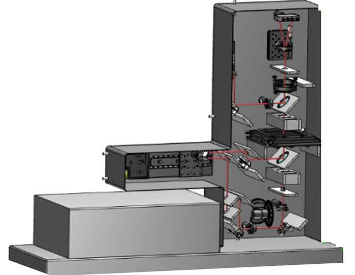
In this project, researchers want to bridge the knowledge gap of fast, non-invasive, and non-destructive semiconductor inspection. They will investigate broadband terahertz (THz - far infrared electromagnetic radiation) spectroscopy, THz emission spectroscopy, microscopy, and nanoscopy in industrially relevant heterogeneous and 2D systems to retrieve material properties as a function of depth and position. With the knowledge gained from this research, together with the industry partners, they will develop a non-invasive and non-destructive prototype based on short pulses of terahertz (THz) radiation in combination with optical pulses to retrieve the properties of as-grown heterogeneous systems in the relevant industrial environment. This prototype will enable material and quality investigations of heterogenous and 2D systems for opto-electronics, micro-electronics and MEMS applications, increasing yield, quality and throughput time all at once, and reducing material waste. This instrument should lead to additional turnover and strengthen the competitiveness of semiconductor foundries.